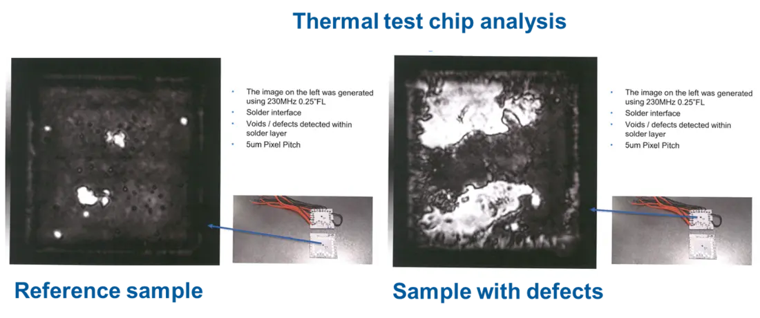
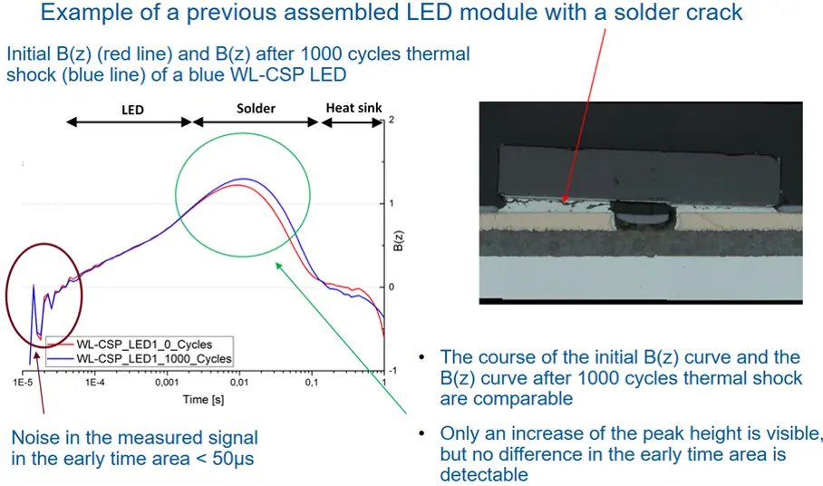
Formation of defects in the bonding material has always been a concern for the reliability of the electronic interconnections. Defects in the bonding materials such as voids and cracks can form either during processing or during the lifetime of the electronic device. These defects not only deteriorate the mechanical strength of the joint they also weaken the electrical and thermal behavior of the electronic device. Thus, the detection of these defects is a major step of microstructural analysis concerning the evaluation of the reliability of the electronic interconnects. Our research group has a key focus on the non-destructive approaches for the detection of the defects in the bonding material. These two approaches are using transient thermal analysis and scanning acoustic microscopy.


1. Transient thermal analysis (TTA)

At our research group, we have developed an automatic panel level TTA tester. The tester targets to ease TTA during reliability assessment and for production inspection. The LED panel is placed on the temperature stabilized table of a xyz-system.

The position of the electrical test pads of the LEDs are read into the machine from Gerber data. The measurement electronics is mounted on the xyz-system to enable the use of short cables with low parasitic inductance. The LEDs are contacted by 4-point probes. To resolve the thermal resistance between the LED die (first level interconnect) and the substrate the forward voltage of the LEDs after current switching need to be measured as early as possible, i.e. well below 10μs. The developed current source allows very fast switching within 100ns and stabilize the detection current within less than 5μs. To evaluate the thermal path and the thermal resistance the relative thermal resistance measurement method is applied.

2. Scanning acoustic microscopy (SAM)

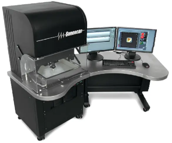
Scanning Acoustic Microscopy (SAM) is a fast, non-invasive and non-destructive investigative technique frequently used in electronic failure analysis. SAM uses ultrasound waves to image interfaces and detect possible defects such as voids, delaminations and cracks within optically opaque structures and components such as chip capacitors, chip resistors, circuit board traces, discrete semiconductor devices, integrated circuits (ICs), and other electronic components.

At our lab we use the SAM equipment mainly to detect delaminations, which are not resolvable under traditional testing methods such as X-ray or computer tomography (CT)-scans. This equipment uses ultrasonic energy (typically 15-100MHz) to scan the objects for defects.

Open positions

If you are interested in vacancies for student work within the research group, please send an email with CV to assistenz-iimo-elger.de.